| CPC H01S 5/18322 (2013.01) [H01S 5/021 (2013.01); H01S 5/0217 (2013.01); H01S 5/0218 (2013.01); H01S 5/02461 (2013.01); H01S 5/1838 (2013.01); H01S 5/18311 (2013.01); H01S 5/18358 (2013.01); H01S 5/18363 (2013.01); H01S 5/3095 (2013.01); H01S 5/34306 (2013.01); H01S 5/34353 (2013.01); H01S 5/04257 (2019.08)] | 17 Claims |
|
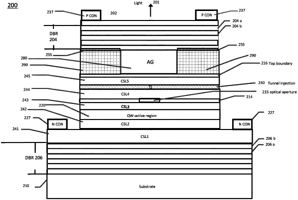
1. A vertical-cavity surface-emitting laser (VCSEL) comprising:
a first substrate;
a first reflector disposed on the first substrate;
a second reflector formed on a gallium arsenide (GaAs) substrate;
an active region structure disposed between the first reflector and the second reflector, wherein the active region structure comprises:
a quantum well structure;
a plurality of current spreading layers;
an aperture layer disposed above the quantum well structure, wherein the aperture layer comprises an optical aperture for a laser light emitted by the VCSEL; and
a tunnel junction layer disposed between the aperture layer and the second reflector;
wherein the active region structure generates a photonic standing wave;
an intermediate layer formed above the active region structure, wherein the intermediate layer comprises a first surface facing the active region structure and a second surface under the second reflector, wherein the intermediate layer contains GaAs, wherein the second surface of the intermediate layer is attached to the second reflector using a GaAs-to-GaAs wafer bonding technique to form a bonding interface;
a eutectic layer disposed on the bonding interface using low temperature bonding to reduce thermal stress caused by the GaAs-to-GaAs wafer bonding;
an air gap formed in the intermediate layer, wherein the air gap opens both the first surface and the second surface of the intermediate layer, and constitutes an optical path from the active region structure to the second reflector;
an interfacial layer formed between a bottom surface of the second reflector and the second surface of the intermediate layer outside the air gap, wherein the interfacial layer does not overlap with the airgap, wherein the interfacial layer is attached to the second surface of the intermediate layer around the air gap;
an N-type electric contact layer patterned adjacent to the active region structure and a P-side electric contact layer patterned on a top surface of the second reflector, connecting to a p-side of the active region structure; and
a VCSEL laser output formed on the top surface of the second reflector;
wherein the air gap, the optical aperture in the aperture layer, and the VSCEL laser output align on one optical axis.
|