| CPC H01Q 21/065 (2013.01) [H01Q 1/2283 (2013.01); H01Q 1/48 (2013.01); H01Q 19/10 (2013.01)] | 23 Claims |
|
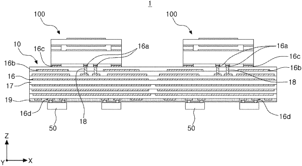
1. A chip antenna module comprising:
a substrate comprising an upper surface pad disposed on a first surface of the substrate and a feed pad disposed on the first surface of the substrate;
a chip antenna configured to transmit a radio-frequency signal, electrically connected to the feed pad, and bonded to the upper surface pad; and
an electronic element mounted on a second surface of the substrate,
wherein the chip antenna comprises:
a first ceramic substrate bonded to the upper surface pad;
a second ceramic substrate opposing the first ceramic substrate;
a first patch disposed on the first ceramic substrate; and
a second patch disposed on the second ceramic substrate, and
the first ceramic substrate and the second ceramic substrate are spaced apart from each other.
|