| CPC H01Q 1/243 (2013.01) [G06F 1/1643 (2013.01); G06F 3/0412 (2013.01); G06F 3/0446 (2019.05)] | 24 Claims |
|
1. An electronic device, comprising:
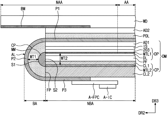
a display module comprising a display area and a non-display area;
an antenna layer disposed on the display module, the antenna layer comprising a bending area at least partially overlapping the non-display area and a non-bending area adjacent to the bending area, the antenna layer further comprising a first portion disposed in the non-bending area and a second portion disposed in the bending area, the second portion being bent; and
a spacer disposed between the second portion and the display module and comprising a metal plate that is bent.
|