| CPC H01L 33/62 (2013.01) [H01L 25/0753 (2013.01); H01L 33/505 (2013.01); H01L 33/32 (2013.01); H01L 2933/0041 (2013.01); H01L 2933/0066 (2013.01)] | 15 Claims |
|
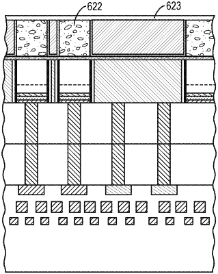
1. A method of making a high-density light emitting diode (LED) display comprising:
depositing a dielectric region overlying a transparent electrically conductive region of an integrated LED array, wherein,
a first portion of the transparent electrically conductive region overlies each of the LEDs and a second portion of the transparent electrically conductive region overlies a metal region; and
a first portion of the dielectric region overlies the first portion of the transparent electrically conductive region and the second portion of the transparent electrically conductive region;
etching the second portion of the dielectric region to expose the transparent electrically conductive region;
depositing a reflective metal region overlying the first portion of the dielectric region and overlying the exposed transparent electrically conductive region;
depositing a metal region overlying the reflective metal region;
planarizing the metal region to expose the first portion of the dielectric region;
etching the first portion of the dielectric region to expose the first portion of the transparent electrically conductive region to provide a cavity overlying each LED; and
filling each of the cavities with a color conversion material to provide a color conversion pixel overlying each of the LEDs.
|