| CPC H01L 33/62 (2013.01) [H01L 23/481 (2013.01); H01L 23/49822 (2013.01); H01L 24/16 (2013.01); H01L 25/167 (2013.01); H01L 2224/16227 (2013.01)] | 19 Claims |
|
1. A LED driving system, comprising:
a LED matrix having a plurality of LED pixels;
a plurality of driver dies/chips, wherein each one of the plurality of driver dies/chips is provided to drive a corresponding predetermined number of LED pixels in the LED matrix, and wherein the predetermined number is an integer greater than 1, and wherein for each individual driver die/chip, an array of discrete pads and at least one common pad are formed on a top surface of the individual driver die/chip, and wherein the array of discrete pads are separated from each other, and wherein the at least one common pad is separated from each one of the array of discrete pads; and
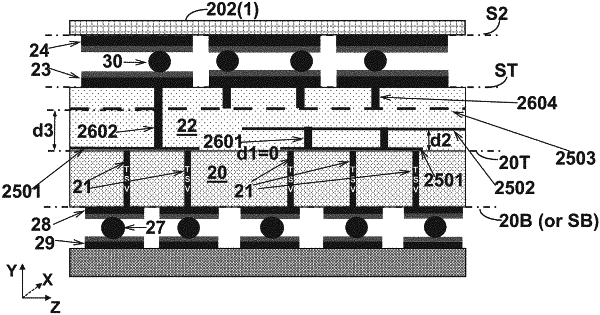
an interconnection structure comprising at least one semiconductor layer having a plurality groups of through semiconductor vias formed in the at least one semiconductor layer and at least one rewiring layer formed on the at least one semiconductor layer, wherein the at least one semiconductor layer has a first surface used as a first surface of the interconnection structure, and wherein the at least one rewiring layer has a surface used as a second surface of the interconnection structure, and wherein the plurality of driver dies/chips are attached to the first surface of the interconnection structure, and wherein the plurality of LED pixels of the LED matrix are attached to the second surface of the interconnection structure, and wherein the interconnection structure is configured to electrically couple each one of the plurality of driver dies/chips to the corresponding predetermined number of LED pixels in the LED matrix.
|