| CPC H01L 33/60 (2013.01) [H01L 27/156 (2013.01); H01L 33/62 (2013.01)] | 20 Claims |
|
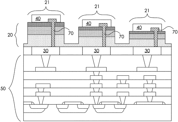
1. A method for manufacturing a reflective structure, the method comprising:
receiving a metallization structure;
forming a first conductive pad, a second conductive pad, and a third conductive pad over the metallization structure; and
forming a plurality of dielectric stacks over the metallization structure, the forming of the plurality of dielectric stacks comprising:
forming a first dielectric stack over the first conductive pad;
forming a second dielectric stack adjacent to the first dielectric stack, the second dielectric stack covering the second conductive pad; and
forming a third dielectric stack adjacent to the second dielectric stack, the third dielectric stack covering the third conductive pad; wherein the thicknesses of the dielectric stacks are different.
|