| CPC H01L 33/405 (2013.01) [H01L 33/22 (2013.01); H01L 33/42 (2013.01); H01L 33/46 (2013.01); H01L 33/62 (2013.01); F21K 9/23 (2016.08); F21K 9/232 (2016.08); F21K 9/69 (2016.08); F21Y 2115/10 (2016.08); H01L 33/0075 (2013.01); H01L 33/06 (2013.01); H01L 33/12 (2013.01); H01L 33/32 (2013.01); H01L 2933/0016 (2013.01); H01L 2933/0025 (2013.01)] | 20 Claims |
|
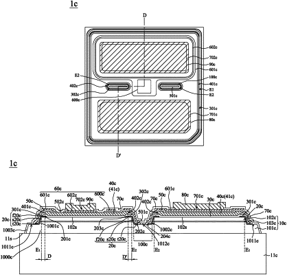
1. A light-emitting device, comprising:
a semiconductor structure comprising a first semiconductor layer, a second semiconductor layer on the first semiconductor layer, and an active layer between the first semiconductor layer and the second semiconductor layer, wherein the second semiconductor layer comprises a first edge;
a reflective structure located on the second semiconductor layer and comprising an outer edge;
a first electrode pad located on the reflective structure, wherein the first electrode pad comprising an outer side wall adjacent to the outer edge,
wherein the outer edge of the reflective structure extends beyond the outer side wall of the first electrode pad and does not exceed and coincide with the first edge of the second semiconductor layer, and the outer edge of the reflective structure is between the outer side wall of the first electrode pad and the first edge of the second semiconductor layer in a cross-sectional view of the light-emitting device.
|