US 11,721,790 B2
Solid state lighting devices with accessible electrodes and methods of manufacturing
Martin F. Schubert, Mountain View, CA (US); and Vladimir Odnoblyudov, Eagle, ID (US)
Assigned to Micron Technology, Inc., Boise, ID (US)
Filed by Micron Technology, Inc., Boise, ID (US)
Filed on Jan. 15, 2021, as Appl. No. 17/150,945.
Application 17/150,945 is a continuation of application No. 16/377,871, filed on Apr. 8, 2019, granted, now 10,896,995.
Application 16/377,871 is a continuation of application No. 15/961,473, filed on Apr. 24, 2018, granted, now 10,256,369, issued on Apr. 9, 2019.
Application 15/961,473 is a continuation of application No. 15/262,956, filed on Sep. 12, 2016, granted, now 9,985,183, issued on May 29, 2018.
Application 15/262,956 is a continuation of application No. 14/614,247, filed on Feb. 4, 2015, granted, now 9,444,014, issued on Sep. 13, 2016.
Application 14/614,247 is a continuation of application No. 13/926,799, filed on Jun. 25, 2013, granted, now 9,000,456, issued on Apr. 7, 2015.
Application 13/926,799 is a continuation of application No. 12/970,726, filed on Dec. 16, 2010, granted, now 8,476,649, issued on Jul. 2, 2013.
Prior Publication US 2021/0135055 A1, May 6, 2021
This patent is subject to a terminal disclaimer.
Int. Cl. H01L 33/38 (2010.01); H01L 33/36 (2010.01); H01L 33/00 (2010.01); H01L 33/06 (2010.01); H01L 33/40 (2010.01); H01L 33/42 (2010.01); H01L 33/62 (2010.01)
CPC H01L 33/382 (2013.01) [H01L 33/0075 (2013.01); H01L 33/06 (2013.01); H01L 33/36 (2013.01); H01L 33/387 (2013.01); H01L 33/405 (2013.01); H01L 33/42 (2013.01); H01L 33/62 (2013.01); H01L 2224/48091 (2013.01); H01L 2224/48137 (2013.01); H01L 2224/49107 (2013.01); H01L 2933/0016 (2013.01)] 20 Claims
OG exemplary drawing
 
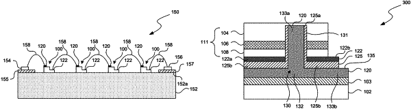
1. A light emitting die, comprising:
a solid state lighting structure including a first semiconductor material, a second semiconductor material, and an active region between the first and second semiconductor materials;
a first electrode disposed on a surface of the first semiconductor material opposite the active region; and
a second electrode extending through the first semiconductor material and the active region and having an end surface contacting the second semiconductor material.