| CPC H01L 33/22 (2013.01) [H01L 33/005 (2013.01); H01L 33/10 (2013.01); H01L 33/382 (2013.01); H01L 2933/0016 (2013.01)] | 19 Claims |

|
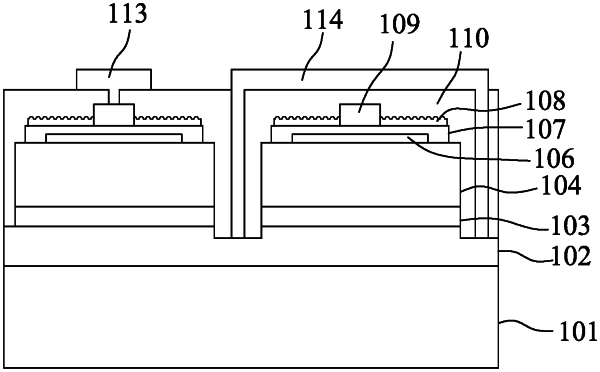
1. A light-emitting diode device, comprising:
a substrate;
an epitaxial layered structure which includes a first-type semiconductor layer, an active layer, and a second-type semiconductor layer sequentially formed on said substrate in such order, and which is formed with an indentation extending through said second-type semiconductor layer and said active layer and terminating at said first-type semiconductor layer to expose a portion of said first-type semiconductor layer;
a first current-blocking layer formed on said epitaxial layered structure opposite to said substrate;
a current-spreading layer which is disposed on said epitaxial layered structure opposite to said substrate, which is disposed over said first current-blocking layer, and which is connected to said epitaxial layered structure;
a second current-blocking layer which is formed on said current-spreading layer opposite to said epitaxial layered structure; and
a distributed Bragg reflector which covers said epitaxial layered structure, said current-spreading layer, and said second current-blocking layer.
|