| CPC H01L 33/12 (2013.01) [H01L 33/005 (2013.01); H01L 33/007 (2013.01); H01L 33/0093 (2020.05); H01L 33/06 (2013.01); H01L 33/32 (2013.01); H01L 33/38 (2013.01); H01L 33/46 (2013.01); H01L 33/62 (2013.01); H01L 2224/16 (2013.01); H01L 2924/1461 (2013.01); H01L 2933/0016 (2013.01); H01L 2933/0025 (2013.01); H01L 2933/0066 (2013.01)] | 6 Claims |
|
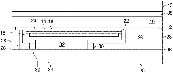
1. A method comprising:
providing a wafer comprising light-emitting devices on a growth substrate, the wafer comprising a first surface and a second surface opposite the first surface, the first surface comprising at least portions of the light-emitting devices and the second surface being a surface of the growth substrate;
bonding the first surface of the wafer to a support wafer at a first above room temperature bonding temperature;
bonding the second surface of the wafer to a stress-compensating wafer at a second above room temperature bonding temperature to form a bonded stack comprising the wafer, the support wafer and the stress-compensating wafer, the support wafer and the stress-compensating wafer having the same thickness and being formed from the same material; and
allowing the bonded stack to cool to room temperature.
|