US 11,721,784 B2
High efficient micro devices
Gholamreza Chaji, Waterloo (CA); Ehsanollah Fathi, Waterloo (CA); and Hossein Zamani Siboni, Waterloo (CA)
Assigned to VueReal Inc., Waterloo (CA)
Filed by VueReal Inc., Waterloo (CA)
Filed on Jun. 28, 2022, as Appl. No. 17/851,622.
Application 17/851,622 is a continuation of application No. 16/428,103, filed on May 31, 2019, granted, now 11,600,743.
Application 16/428,103 is a continuation in part of application No. 15/942,154, filed on Mar. 30, 2018, abandoned.
Claims priority of provisional application 62/684,677, filed on Jun. 13, 2018.
Claims priority of provisional application 62/682,479, filed on Jun. 8, 2018.
Claims priority of provisional application 62/533,394, filed on Jul. 17, 2017.
Claims priority of provisional application 62/479,038, filed on Mar. 30, 2017.
Prior Publication US 2022/0328715 A1, Oct. 13, 2022
Int. Cl. H01L 25/16 (2023.01); H01L 29/40 (2006.01); H01L 33/00 (2010.01); H01L 29/423 (2006.01); H01L 33/44 (2010.01); H01L 27/15 (2006.01); H01L 33/20 (2010.01)
CPC H01L 33/0041 (2013.01) [H01L 25/167 (2013.01); H01L 29/401 (2013.01); H01L 29/42312 (2013.01); H01L 33/0037 (2013.01); H01L 27/156 (2013.01); H01L 33/007 (2013.01); H01L 33/0093 (2020.05); H01L 33/20 (2013.01); H01L 33/44 (2013.01); H01L 2933/0066 (2013.01)] 2 Claims
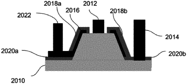
OG exemplary drawing
 
1. A method to bias an edge of a micro device:
covering at least part of the edge of the micro device with a metal-insulator-semiconductor (MIS) structure, wherein the MIS structure comprises a stack of dielectric layers and a MIS gate conductive layer; and
creating intrinsic potential biasing the edge of the micro device using different dielectric layers with a different band structure.