| CPC H01L 31/202 (2013.01) [H01L 31/02167 (2013.01); H01L 31/022425 (2013.01); H01L 31/0747 (2013.01); H01L 31/1864 (2013.01); H01L 31/208 (2013.01)] | 19 Claims |
|
1. A solar cell, comprising:
a semiconductor substrate having a front side and a back side opposite to each other;
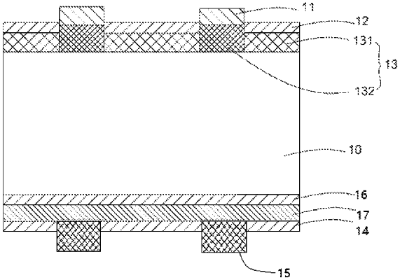
a doped layer located on the front side of the semiconductor substrate, wherein the doped layer has a lightly doped region having a first doping concentration and a heavily doped region having a second doping concentration greater than the first doping concentration, and the heavily doped region protrudes from a surface of the semiconductor substrate and includes doped polycrystalline silicon;
a front passivated layer and/or a anti-reflection layer located on a surface of the doped layer facing away from the semiconductor substrate; and
a front electrode located on a surface of the front passivated layer and/or the anti-reflection layer facing away from the doped layer, wherein the front electrode penetrates through the front passivated layer and/or the anti-reflection layer to form an ohmic contact with the heavily doped region of the doped layer,
wherein the solar cell further comprises:
a tunnel oxidized layer located on the back side of the semiconductor substrate;
a doped amorphous silicon layer located on a surface of the tunnel oxidized layer facing away from the semiconductor substrate;
a back passivated layer located on a surface of the doped amorphous silicon layer facing away from the tunnel oxidized layer; and
a back electrode located on a surface of the back passivated layer facing away from the doped amorphous silicon layer, wherein the back electrode penetrates through the back passivated layer to form an ohmic contact with the doped amorphous silicon layer.
|