| CPC H01L 31/1075 (2013.01) [H01L 31/028 (2013.01); H01L 31/035281 (2013.01); H01L 31/1804 (2013.01)] | 20 Claims |
|
1. A structure for an avalanche photodetector, the structure comprising:
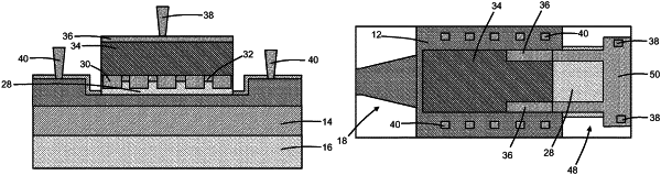
a first semiconductor layer including a first portion and a second portion, the first portion of the first semiconductor layer defining a multiplication region of the avalanche photodetector;
a second semiconductor layer stacked in a vertical direction with the first semiconductor layer, the second semiconductor layer defining an absorption region of the avalanche photodetector;
a charge sheet in the second portion of the first semiconductor layer, the charge sheet having a thickness that varies with position in a horizontal plane, the charge sheet positioned in the vertical direction between the second semiconductor layer and the first portion of the first semiconductor layer, the charge sheet including a first plurality of doped regions and a doped layer superimposed on the first plurality of doped regions, the first plurality of doped regions and the doped layer each containing a dopant of a first conductivity type, the first plurality of doped regions having a first thickness, and the doped layer having a second thickness that is less than the first thickness; and
a pad comprising a semiconductor material having a second conductivity type different than the first conductivity type,
wherein the first semiconductor layer and the second semiconductor layer are positioned on the pad.
|