| CPC H01L 31/0508 (2013.01) [H01L 31/0488 (2013.01); H01L 31/0512 (2013.01); H01L 31/0547 (2014.12)] | 10 Claims |
|
1. A photovoltaic module, comprising:
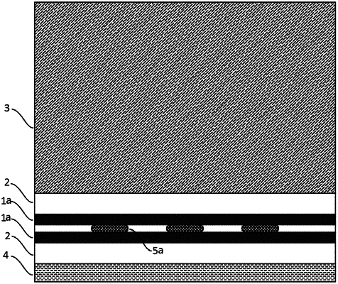
a solar cell string comprising a plurality of solar cells, adjacent two of the plurality of solar cells being connected by a solder strip, wherein the solder strip is connected to a front surface of one solar cell and to a back surface of another solar cell, and a long-side size of the solar cell is within a range of 150 mm to 220 mm;
two protective adhesive layers respectively covering a front surface and a back surface of the solar cell string, wherein a size difference between a thickness of one protective adhesive layer and a thickness of the solder strip is defined as a first thickness, a ratio of the first thickness to the thickness of one protective adhesive layer is not less than 5% and not greater than 15%;
a transparent plate covering a surface of the protective adhesive layer on the front surface of the solar cell string; and
a back plate covering a surface of the protective adhesive layer on the back surface of the solar cell string;
each of the plurality of solar cells comprises a single-layer region and an overlapping region, and adjacent two of the solar cells are stacked in the overlapping region, and the protective adhesive layer has a gram weight of 245 g/m2 to 430 g/m2;
the solder strip comprises a reflective section and a flat section connected to the reflective section, the reflective section is arranged in the single-layer region, and the flat section is at least partially arranged in the overlapping region; and
a cross section of the flat section is a cashew-shaped surface, and the cashew-shaped surface is defined by planar regions on both sides of the solder strip in a thickness direction and arc-shaped regions on both sides of the solder strip in a width direction.
|