| CPC H01L 31/03042 (2013.01) [H01L 27/14643 (2013.01); H01L 27/14698 (2013.01); H01L 31/03529 (2013.01); H01L 31/1035 (2013.01); H01L 31/1864 (2013.01)] | 20 Claims |
|
1. A method for forming an image sensor, the method comprising:
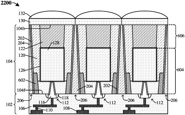
performing a first ion implantation process on a front-side surface of a semiconductor substrate to form first doped regions within the semiconductor substrate, wherein the first doped regions comprise a first dopant having a first doping type;
forming a second doped region within the semiconductor substrate such that the second doped region abuts the first doped regions, wherein the second doped region comprises a second dopant having a second doping type opposite the first doping type, wherein the second dopant comprises gallium, wherein forming the second doped region comprises:
patterning the front-side surface of the semiconductor substrate to form an opening within the semiconductor substrate;
forming a doped liner along sidewalls and a lower surface of the semiconductor substrate that define the opening, wherein the doped liner comprises the second dopant, wherein the doped liner is formed before forming the second doped region;
performing an annealing process on the semiconductor substrate, thereby forming the second doped region within the semiconductor substrate, wherein the annealing process drives the second dopant from the doped liner into the semiconductor substrate; and
forming a plurality of semiconductor devices along the front-side surface of the semiconductor substrate.
|