| CPC H01L 29/945 (2013.01) [H01L 21/2652 (2013.01); H01L 28/91 (2013.01); H01L 29/40114 (2019.08); H01L 29/4236 (2013.01); H01L 29/788 (2013.01); H10B 41/35 (2023.02)] | 32 Claims |
|
1. An integrated circuit, comprising:
a semiconductor substrate including a plurality of excavations in the form of trenches sunk into the semiconductor substrate substantially perpendicularly to a front face of the semiconductor substrate;
wherein said trenches each have a depth in the semiconductor substrate that is explicitly between 500 nn and 1200 nm;
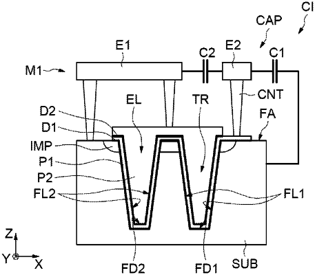
a non-volatile memory cell including a floating gate and a control gate; and
at least one capacitive element comprising:
a first dielectric envelope covering a part of the front face and conforming to sides and bottoms of the trenches, said first dielectric envelope and a tunnel dielectric for the floating gate being formed by a first conjoint dielectric layer;
a first semiconductor layer on the first dielectric envelope, covering part of the front face and conforming to a surface of the first dielectric envelope inside each trench, said first semiconductor layer and floating gate being formed by a first conjoint semiconductor layer;
a second dielectric envelope on the first semiconductor layer, covering part of the front face and conforming to a surface of the first semiconductor layer inside each trench, said second dielectric envelope and a dielectric for the control gate being formed by a second conjoint dielectric layer; and
a second semiconductor layer on the second dielectric envelope, covering part of the front face, said second semiconductor layer and control gate being formed by a second conjoint semiconductor layer.
|