| CPC H01L 29/7869 (2013.01) [H01L 27/1251 (2013.01); H01L 29/105 (2013.01); H01L 29/24 (2013.01)] | 23 Claims |
|
1. A transistor comprising:
a gate electrode;
an active layer facing the gate electrode; and
a source electrode and a drain electrode connected to the active layer,
wherein the active layer includes:
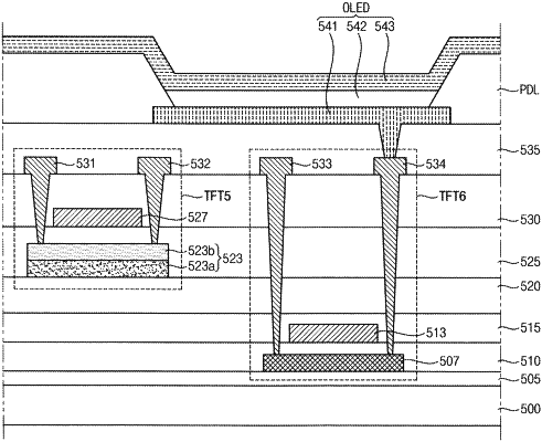
a lower active layer and an upper active layer which face each other and each include an oxide semiconductor material,
the upper active layer closer to the source electrode and the drain electrode than the lower active layer and further including an oxygen-gettering material,
the lower active layer excluding the oxygen-gettering material, and
each of the lower active layer and the upper active layer having a thickness,
wherein the thickness of the lower active layer is different from the thickness of the upper active layer.
|