| CPC H01L 29/7869 (2013.01) [H01L 21/02565 (2013.01); H01L 21/477 (2013.01); H01L 29/24 (2013.01); H01L 29/517 (2013.01); H01L 29/66969 (2013.01); H01L 29/78642 (2013.01)] | 20 Claims |
|
1. A transistor comprising:
a gate electrode;
a dielectric layer;
source and drain electrodes; and
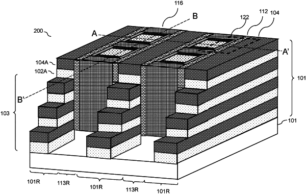
a channel layer having an upper surface, a lower surface, and a middle portion between the upper surface and the lower surface, wherein the source and drain electrodes electrically contact the upper surface of the channel layer and the channel layer has a first carrier concentration proximate to the upper surface of the channel layer, a second carrier concentration in the middle portion of the channel layer, a third carrier concentration proximate to the lower surface of the channel layer, and the first carrier concentration is less than the second carrier concentration and the third carrier concentration is less than the second carrier concentration, and wherein the channel layer comprises:
a first oxide semiconductor layer having a first oxygen concentration;
a second oxide semiconductor layer having a second oxygen concentration; and
a third oxide semiconductor layer having a third oxygen concentration,
wherein the second oxide semiconductor layer is located between the first oxide semiconductor layer and the third oxide semiconductor layer; and
wherein the second oxygen concentration is lower than the first oxygen concentration and the third oxygen concentration, and
a thickness of the second oxide semiconductor layer is greater than a combined thickness of the first oxide semiconductor layer and the third oxide semiconductor layer.
|