| CPC H01L 29/78627 (2013.01) [H01L 21/02178 (2013.01); H01L 21/02565 (2013.01); H01L 21/426 (2013.01); H01L 21/47573 (2013.01); H01L 21/47635 (2013.01); H01L 27/124 (2013.01); H01L 27/127 (2013.01); H01L 27/1225 (2013.01); H01L 27/1251 (2013.01); H01L 29/24 (2013.01); H01L 29/42384 (2013.01); H01L 29/4908 (2013.01); H01L 29/66969 (2013.01); H01L 29/7869 (2013.01); H01L 29/78633 (2013.01); H01L 29/78675 (2013.01); G02F 1/1368 (2013.01); H01L 2029/42388 (2013.01)] | 5 Claims |
|
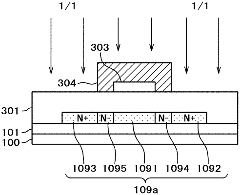
1. A method of manufacturing a semiconductor device with a thin film transistor having an oxide semiconductor which includes a channel region, a drain region, a source region, and low concentration regions which are lower in impurity concentration than the drain region and the source region, the low concentration regions being located between the channel region and the drain region, and between the channel region and the source region, comprising steps of:
selectively forming a semiconductor layer of the thin film transistor on a substrate;
forming a gate insulating film so as to cover the semiconductor layer;
forming an aluminum oxide film on the gate insulating film;
selectively patterning the aluminum oxide film so as to be locate on the channel region;
forming a gate electrode on the gate insulating film and on the aluminum oxide film selectively patterned;
selectively patterning the gate electrode so as to be located on the aluminum oxide film selectively patterned and on the low concentration regions; and
performing ion implantation by using the gate electrode selectively patterned as a mask.
|