| CPC H01L 29/7851 (2013.01) [H01L 21/76804 (2013.01); H01L 21/76831 (2013.01); H01L 21/76897 (2013.01); H01L 23/5226 (2013.01); H01L 23/5283 (2013.01); H01L 29/41766 (2013.01); H01L 29/41791 (2013.01); H01L 29/66545 (2013.01); H01L 29/66795 (2013.01); H01L 23/485 (2013.01); H01L 29/165 (2013.01); H01L 29/7848 (2013.01); H01L 2029/7858 (2013.01)] | 20 Claims |
|
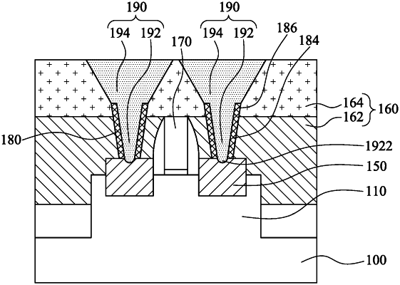
1. A method, comprising:
forming a source/drain region on a substrate;
forming a dielectric layer over the source/drain region;
forming a contact hole in the dielectric layer;
forming a contact hole liner in the contact hole;
removing a first portion of the contact hole liner to expose a sidewall of the contact hole in a first etching step, wherein the first etching step also removes a portion of the contact hole liner to expose the source/drain region;
performing a second etching step to recess the source/drain region, wherein the second etching step also etches the exposed sidewall of the contact hole to laterally expand the contact hole; and
forming a contact plug in the laterally expanded contact hole.
|