| CPC H01L 29/7802 (2013.01) [H01L 29/1608 (2013.01); H01L 29/7833 (2013.01)] | 26 Claims |
|
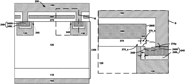
1. A method of forming a semiconductor device, comprising:
providing a drift layer on a substrate, the drift layer comprising a surface opposite the substrate;
implanting ions into the drift layer to form a source/drain region in an upper portion of the drift layer that has a first portion that has a first dopant dose and a second portion in the first portion, the second portion having a second dopant dose, different from the first dopant dose;
forming a gate dielectric layer on the drift layer; and
forming a gate electrode on the gate dielectric layer, the gate electrode is entirely above the surface of the drift layer,
wherein a portion of the gate dielectric layer has a bottom surface that is closer to the substrate than a top surface of the first portion of the source/drain region.
|