| CPC H01L 29/7787 (2013.01) [H01L 21/0251 (2013.01); H01L 21/0254 (2013.01); H01L 21/0262 (2013.01); H01L 21/02458 (2013.01); H01L 21/02579 (2013.01); H01L 29/2003 (2013.01); H01L 29/66462 (2013.01); H01L 21/26546 (2013.01)] | 20 Claims |
|
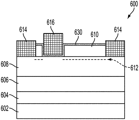
1. A semiconductor device comprising:
a doped substrate;
a seed layer in direct contact with the substrate, wherein the seed layer comprises:
a first seed sublayer having a first lattice structure, wherein the first seed sublayer comprises AlN, and the first seed sublayer is doped with carbon, and
a second seed sublayer over the first seed layer, wherein the second seed layer has a second lattice structure different from the first lattice structure, and a thickness of the second seed sublayer ranges from about 50 nanometers (nm) to about 200 nm;
a graded layer in direct contact with the seed layer, wherein the graded layer comprises:
a first graded sublayer including AlGaN, wherein the first graded sublayer has a first Al:Ga ratio;
a second graded sublayer over the first graded sublayer, wherein the second graded sublayer includes AlGaN, and the second graded sublayer has a second Al:Ga ratio different from the first Al:Ga ratio; and
a third graded sublayer over the second graded sublayer, wherein the third graded sub layer includes AlGaN, and the third graded sublayer has a third Al:Ga ratio different from the second Al:Ga ratio;
a channel layer over the graded layer, wherein a two-dimensional electron gas (2-DEG) is defined in the channel layer; and
an active layer over the channel layer.
|