| CPC H01L 29/7397 (2013.01) [H01L 29/1095 (2013.01); H01L 29/41708 (2013.01)] | 18 Claims |
|
1. A semiconductor device, comprising:
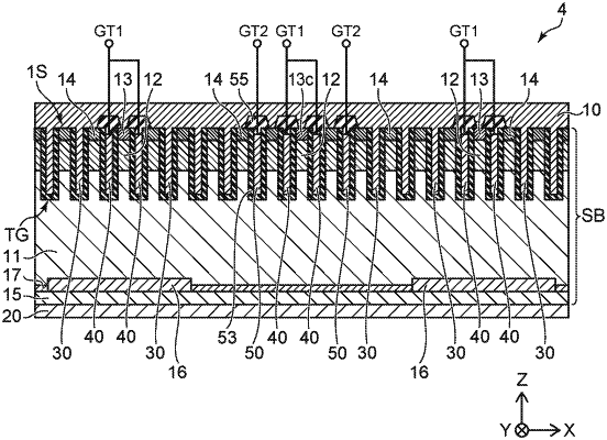
a semiconductor part including a first semiconductor layer of a first conductivity type, a second semiconductor layer of a second conductivity type, a third semiconductor layer of the first conductivity type, at least one fourth semiconductor layer of the second conductivity type, a fifth semiconductor layer of the second conductivity type, at least one sixth semiconductor layer of the first conductivity type, a seventh semiconductor layer of the first conductivity type, the semiconductor part having a first surface and a second surface at a side opposite to the first surface;
a first electrode provided on the first surface of the semiconductor part, the second semiconductor layer being provided between the first semiconductor layer and the first electrode, the third and fourth semiconductor layers being provided between the second semiconductor layer and the first electrode, the first electrode being electrically connected to the third and fourth semiconductor layers, the third and fourth semiconductor layers being arranged along the first surface of the semiconductor part;
a second electrode provided on the second surface of the semiconductor part, the semiconductor part being provided between the first electrode and the second electrode, the first semiconductor layer extending between the first electrode and the second electrode, the fifth semiconductor layer being provided between the second electrode and the first semiconductor layer, the fifth semiconductor layer being electrically connected to the second electrode, the sixth and seventh semiconductor layers being provided between the first and fifth semiconductor layers, the sixth and seventh semiconductor layers being arranged along the fifth semiconductor layer, the sixth and seventh semiconductor layers including a first-conductivity-type impurity with higher concentrations than a concentration of a first-conductivity-type impurity in the first semiconductor layer, the sixth semiconductor layer including the first-conductivity-type impurity with a first surface density in a plane parallel to the second surface, the seventh semiconductor layer including the first-conductivity-type impurity with a second surface density in the plane parallel to the second surface, the first surface density being greater than the second surface density, the seventh semiconductor layer being provided between two adjacent portions of the sixth semiconductor layer, or between the sixth semiconductor layer and another sixth semiconductor layer; and
at least one control electrode provided between the semiconductor part and the first electrode, the control electrode being electrically insulated from the semiconductor part by a first insulating film and electrically insulated from the first electrode by a second insulating film, the control electrode facing the first and second semiconductor layers via the first insulating film, the first to third semiconductor layers being arranged along the first insulating film.
|