| CPC H01L 29/7395 (2013.01) [H01L 27/0629 (2013.01); H01L 29/0821 (2013.01); H01L 29/7889 (2013.01)] | 5 Claims |
|
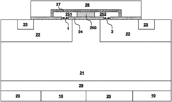
1. An insulated gate bipolar transistor (IGBT) power device, comprising:
an n-type collector region and a p-type collector region, an n-type drift region located above the n-type collector region and the p-type collector region, at least two p-type body regions located at a top of the n-type drift region, wherein two p-type body regions of the at least two p-type body regions are isolated by the n-type drift region; and an n-type emitter region located within each p-type body region of the at least two p-type body regions;
a gate dielectric layer located above the two p-type body regions and the n-type drift region between the two p-type body regions, an n-type floating gate located above the gate dielectric layer; a gate located above the gate dielectric layer and the n-type floating gate, wherein the gate covers two side walls of the n-type floating gate in a lateral direction; and an insulating dielectric layer between the gate and the n-type floating gate;
a first opening located in the gate dielectric layer, wherein the n-type floating gate in contact with one p-type body region of the two p-type body regions through the first opening to form a p-n junction diode; and
a second opening located in the gate dielectric layer, wherein the n-type floating gate is in contact with the other p-type body region of the two p-type body regions through the second opening to form a p-n junction diode.
|