| CPC H01L 29/66666 (2013.01) [H01L 29/6653 (2013.01); H01L 29/66545 (2013.01); H01L 21/0245 (2013.01); H01L 21/02483 (2013.01); H01L 21/02507 (2013.01); H01L 21/02532 (2013.01); H01L 21/02565 (2013.01); H01L 21/02639 (2013.01)] | 13 Claims |
|
1. A method of making a three-dimensional semiconductor structure, comprising:
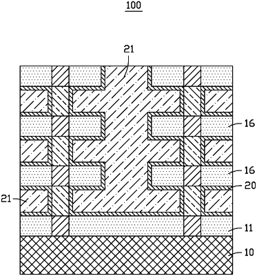
providing a substrate, forming a first insulating layer on the substrate, and defining at least one channel hole in the first insulating layer, wherein each channel hole extends through the first insulating layer and exposes the substrate;
forming a first epitaxial layer and a second epitaxial layer stacked on the first epitaxial layer in each channel hole, the first epitaxial layer being configured to form a source region or a drain region;
forming a sacrificial layer on the first insulating layer and exposing the second epitaxial layer relative to the sacrificial layer, forming another first epitaxial layer stacking on the second epitaxial layer; forming a second insulating layer on the sacrificial layer and exposing the another first epitaxial layer relative to the second insulating layer, and forming another second epitaxial layer stacking on the another first epitaxial layer;
repeating previous steps to totally form a plurality of sacrificial layers and a plurality of second insulating layers alternately stacked on the first insulating layer, and totally form a plurality of first epitaxial layers and a plurality of second epitaxial layers alternately stacked on the substrate.
|