US 11,721,742 B2
Memory modules and memory packages including graphene layers for thermal management
Chan H. Yoo, Boise, ID (US); George E. Pax, Boise, ID (US); Yogesh Sharma, Boise, ID (US); Gregory A. King, Hastings, MN (US); Thomas H. Kinsley, Boise, ID (US); and Randon K. Richards, Kuna, ID (US)
Assigned to Micron Technology, Inc., Boise, ID (US)
Filed by Micron Technology, Inc., Boise, ID (US)
Filed on Aug. 2, 2021, as Appl. No. 17/391,920.
Application 17/391,920 is a continuation of application No. 16/530,757, filed on Aug. 2, 2019, granted, now 11,081,565.
Prior Publication US 2021/0367057 A1, Nov. 25, 2021
Int. Cl. H05K 1/18 (2006.01); H01L 29/66 (2006.01); H01L 23/495 (2006.01); H05K 1/11 (2006.01); H01L 23/14 (2006.01)
CPC H01L 29/66015 (2013.01) [H01L 23/145 (2013.01); H01L 23/49506 (2013.01); H01L 23/49513 (2013.01); H05K 1/117 (2013.01); H05K 1/181 (2013.01)] 19 Claims
OG exemplary drawing
 
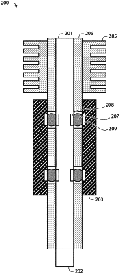
1. An apparatus, comprising:
a substrate having a layer of graphene that comprises a plurality of openings corresponding to a plurality of substrate pads; and
a die disposed over the substrate and having a plurality of electrical connections, each of the plurality of electrical connections in contact with a corresponding one of the plurality of substrate pads,
wherein the layer of graphene is in contact with the die.