| CPC H01L 29/4983 (2013.01) [H01L 21/28123 (2013.01); H01L 29/0673 (2013.01); H01L 29/0847 (2013.01); H01L 29/42392 (2013.01); H01L 29/66545 (2013.01); H01L 29/66795 (2013.01); H01L 29/7851 (2013.01); H01L 29/78618 (2013.01); H01L 29/78696 (2013.01)] | 20 Claims |
|
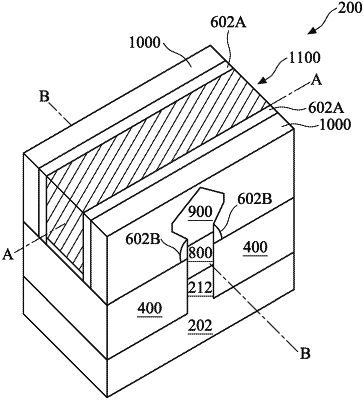
1. A semiconductor device, comprising:
a substrate;
a semiconductor fin over the substrate and laterally extending along a first axis;
a first source/drain region extending from a first end of the semiconductor fin along the first axis;
a second source/drain region extending from a second end of the semiconductor fin along the first axis;
a first dielectric structure extending vertically below a lower surface of a gate dielectric layer disposed laterally between the first dielectric structure and a second dielectric structure;
the second dielectric structure extending vertically below the lower surface of the gate dielectric layer, wherein the first source/drain region and the second source/drain region are vertically elevated from an upper surface of the gate dielectric layer by the first and second dielectric structures, respectively;
a first isolation region disposed on a first side of a lower portion of the semiconductor fin along a second axis; and
a second isolation region disposed on a second side of the lower portion of the semiconductor fin along the second axis.
|