US 11,721,740 B2
Semiconductor device and method of manufacturing the same
Jui-Fen Chien, Taichung (TW); Hsiao-Kuan Wei, Taoyuan County (TW); Hsien-Ming Lee, Changhua (TW); and Chin-You Hsu, Hsinchu (TW)
Assigned to Taiwan Semiconductor Manufacturing Company, Ltd., Hsinchu (TW)
Filed by Taiwan Semiconductor Manufacturing Company, Ltd., Hsinchu (TW)
Filed on Aug. 9, 2021, as Appl. No. 17/396,783.
Application 17/396,783 is a continuation of application No. 16/884,053, filed on May 27, 2020, granted, now 11,088,257.
Application 16/884,053 is a continuation of application No. 15/877,391, filed on Jan. 23, 2018, granted, now 10,707,318, issued on Jul. 7, 2020.
Claims priority of provisional application 62/586,194, filed on Nov. 15, 2017.
Prior Publication US 2021/0367056 A1, Nov. 25, 2021
Int. Cl. H01L 29/78 (2006.01); H01L 29/49 (2006.01); H01L 29/06 (2006.01); H01L 27/092 (2006.01); H01L 29/66 (2006.01); H01L 21/28 (2006.01); H01L 29/165 (2006.01)
CPC H01L 29/4966 (2013.01) [H01L 21/28088 (2013.01); H01L 27/0924 (2013.01); H01L 29/0653 (2013.01); H01L 29/66545 (2013.01); H01L 29/66795 (2013.01); H01L 29/785 (2013.01); H01L 29/7848 (2013.01); H01L 29/165 (2013.01)] 20 Claims
OG exemplary drawing
 
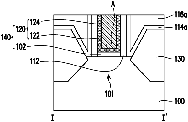
1. A semiconductor device, comprising:
a first n-type transistor comprising a first work function layer, the first work function layer comprising a first underlying layer; and
a second n-type transistor comprising a second work function layer, the second work function layer comprising a second underlying layer,
wherein the first and second underlying layers each comprises a metal nitride layer with at least two kinds of metals, and a thickness of the first underlying layer is greater than a thickness of the second underlying layer.