| CPC H01L 29/4236 (2013.01) [H01L 21/76224 (2013.01); H01L 29/1095 (2013.01); H01L 29/66734 (2013.01); H01L 29/7813 (2013.01)] | 20 Claims |
|
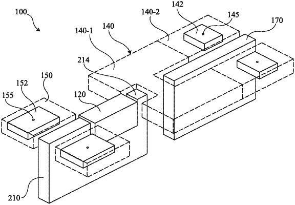
1. A transistor comprising:
a semiconductor drain region delimited by three sides of a first trench;
a first electrically conductive element located in the first trench; and
a first node electrically coupled to the first electrically conductive element, the first node configured to be coupled to a first potential closer to a drain potential of the transistor than to a source potential of the transistor.
|