| CPC H01L 29/41741 (2013.01) [H01L 23/5226 (2013.01); H01L 23/5283 (2013.01); H01L 29/40114 (2019.08); H01L 29/40117 (2019.08); H10B 41/10 (2023.02); H10B 41/27 (2023.02); H10B 41/35 (2023.02); H10B 41/41 (2023.02); H10B 43/10 (2023.02); H10B 43/27 (2023.02); H10B 43/35 (2023.02); H10B 43/40 (2023.02)] | 2 Claims |
|
1. A memory device, comprising:
semiconductor devices located over a substrate;
lower-level metal interconnect structures electrically connected to a respective one of the semiconductor devices and embedded within lower-level dielectric material layers;
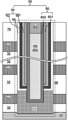
a source contact layer overlying the lower-level dielectric material layers, wherein the source contact layer comprises a silicon-germanium source contact layer;
an alternating stack of insulating layers and electrically conductive layers located over the source contact layer; and
a memory stack structure vertically extending through the alternating stack, wherein the memory stack structure comprises a memory film and a silicon-germanium vertical semiconductor channel that contacts the memory film, and the source contact layer contacts a cylindrical portion of an outer sidewall of the vertical semiconductor channel;
a first source-level silicon-germanium layer located between the lower-level dielectric material layers and the silicon-germanium source contact layer and in contact with a bottom surface of the silicon-germanium source contact layer; and
a dielectric cap structure including a stack of at least a first dielectric plate and a second dielectric plate, wherein the dielectric cap structure is embedded within the first source-level silicon-germanium layer and underlies the vertical semiconductor channel.
|