| CPC H01L 29/165 (2013.01) [H01L 29/0808 (2013.01); H01L 29/1008 (2013.01); H01L 29/401 (2013.01); H01L 29/41708 (2013.01); H01L 29/66242 (2013.01); H01L 29/735 (2013.01); H01L 29/737 (2013.01); H01L 21/8249 (2013.01); H01L 29/66545 (2013.01)] | 6 Claims |
|
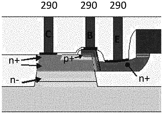
1. A semiconductor device comprising
a semiconductor substrate of a first conductivity type defining a wafer plane parallel to said semiconductor substrate, wherein the semiconductor substrate is a silicon substrate;
a collector region of a second conductivity type disposed on top of said semiconductor substrate, said collector region comprising an n-hill layered structure layer having a top surface and a perimeter in the wafer plane, said n-hill layered structure layer having a base-facing sidewall inclined at an acute angle to said wafer plane along at least a portion of said perimeter;
a base region comprising at least one doped layer of said first conductivity type, said at least one doped layer forming a first metallurgical junction with said collector region, said first metallurgical junction having a portion that is substantially flat;
an emitter region forming a second metallurgical junction with said base region, said second metallurgical junction having a portion that substantially flat, said emitter region comprising a heavily doped layer of said second conductivity type disposed on an isolating layer;
said flat portion of said first metallurgical junction and said flat portion of said second metallurgical junction are substantially parallel to each other and close an acute angle with said wafer plane;
wherein said base region is disposed on a portion of said base-facing sidewall and at least a portion of said base region comprises silicon-germanium alloy or silicon-germanium-carbon alloy.
|