US 11,721,724 B2
Quantum well stacks for quantum dot devices
Nicole K. Thomas, Portland, OR (US); James S. Clarke, Portland, OR (US); Jessica M. Torres, Portland, OR (US); Ravi Pillarisetty, Portland, OR (US); Kanwaljit Singh, Rotterdam (NL); Payam Amin, Portland, OR (US); Hubert C. George, Portland, OR (US); Jeanette M. Roberts, North Plains, OR (US); Roman Caudillo, Portland, OR (US); David J. Michalak, Portland, OR (US); Zachary R. Yoscovits, Beaverton, OR (US); and Lester Lampert, Portland, OR (US)
Assigned to Intel Corporation, Santa Clara, CA (US)
Filed by Intel Corporation, Santa Clara, CA (US)
Filed on Jul. 1, 2021, as Appl. No. 17/364,985.
Application 17/364,985 is a continuation of application No. 16/648,442, granted, now 11,114,530, previously published as PCT/US2017/066894, filed on Dec. 17, 2017.
Prior Publication US 2021/0328019 A1, Oct. 21, 2021
This patent is subject to a terminal disclaimer.
Int. Cl. H01L 29/12 (2006.01); H01L 21/8234 (2006.01); H01L 27/088 (2006.01); H01L 29/66 (2006.01); H01L 29/82 (2006.01)
CPC H01L 29/122 (2013.01) [H01L 21/823431 (2013.01); H01L 27/0886 (2013.01); H01L 29/66977 (2013.01); H01L 29/66984 (2013.01); H01L 29/82 (2013.01)] 20 Claims
OG exemplary drawing
 
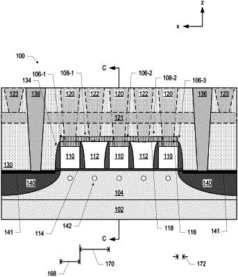
1. A quantum dot device, comprising:
a quantum well stack including a quantum well layer, wherein the quantum well layer includes a material that includes silicon and germanium; and
a gate above the quantum well stack,
wherein the silicon includes 29Si in an amount less than 4 atomic-percent and the germanium includes 73Ge in an amount less than 7 atomic-percent.