| CPC H01L 27/14634 (2013.01) [H01L 21/76898 (2013.01); H01L 23/481 (2013.01); H01L 27/1464 (2013.01); H01L 27/1469 (2013.01); H01L 27/14612 (2013.01); H01L 27/14621 (2013.01); H01L 27/14627 (2013.01); H01L 27/14632 (2013.01); H01L 27/14636 (2013.01); H01L 27/14643 (2013.01); H01L 27/14645 (2013.01); H01L 27/14687 (2013.01); H04N 23/00 (2023.01); H04N 25/76 (2023.01); H04N 25/79 (2023.01); H01L 2224/11 (2013.01)] | 23 Claims |
|
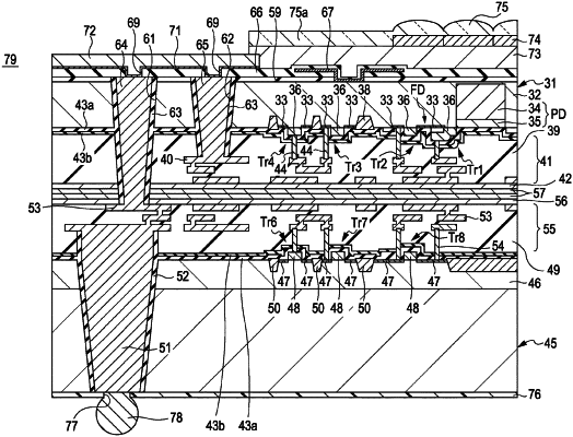
1. A light detecting device, comprising:
a first semiconductor section including a first multi-wiring layer and a photodiode, wherein the first multi-wiring layer is on a side of the first semiconductor section opposite to a light incident side of the first semiconductor section, and wherein the first multi-wiring layer includes a first plurality of wiring layers and a first insulating interlayer; and
a second semiconductor section including a second multi-wiring layer and a circuit, wherein the second multi-wiring layer includes a second plurality of wiring layers and a second insulating interlayer,
wherein the first semiconductor section and the second semiconductor section are bonded together such that the first multi-wiring layer and the second multi-wiring layer face one another,
wherein a first wiring included in the first plurality of wiring layers and a second wiring included in the second plurality of wiring layers are connected to each other,
wherein a first part of the first insulating interlayer and a first part of the second insulating interlayer are connected to each other,
wherein the first wiring is electrically connected to the photodiode,
wherein the second wiring is electrically connected to the circuit, and
wherein the first plurality of wiring layers includes a third wiring, the first wiring and the third wiring are disposed in different layers, and a second part of the first insulating interlayer is disposed between the first wiring and the third wiring.
|