| CPC H01L 27/1463 (2013.01) [H01L 27/1464 (2013.01); H01L 27/1469 (2013.01); H01L 27/14634 (2013.01); H01L 27/14641 (2013.01)] | 20 Claims |
|
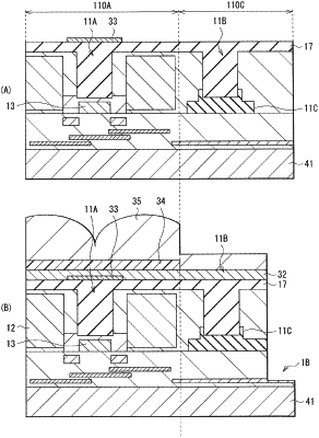
1. An imaging device comprising:
a semiconductor substrate comprising a light-receiving region and a peripheral region, the light-receiving region including a photoelectric conversion region;
a first separation region disposed in the light-receiving region;
a second separation region disposed in the peripheral region; and
a third separation region disposed in the peripheral region and disposed under the second separation region in the semiconductor substrate,
wherein the third separation region includes a first portion, a second portion, and a third portion in a cross-sectional view,
wherein the second separation region is disposed between the first portion and the third portion in the cross-sectional view,
wherein the second separation region contacts with the second portion of the third separation region, and
wherein a width of the first portion is different than a width of the third portion in the cross-sectional view.
|