| CPC H01L 27/14627 (2013.01) [H01L 27/1464 (2013.01); H01L 27/14636 (2013.01); H04N 25/772 (2023.01)] | 20 Claims |
|
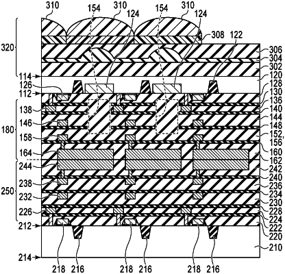
1. A photoelectric conversion device comprising:
a semiconductor layer in which a photoelectric converter is provided;
a substrate arranged on one face side of the semiconductor layer; and
an interconnection structure arranged between the semiconductor layer and the substrate,
wherein light enters the photoelectric converter from another face side of the semiconductor layer,
wherein the interconnection structure includes at least one first insulating film made of a first insulating material, at least one second insulating film provided between the semiconductor layer and the first insulating film and made of a second insulating material, and a plurality of interconnection layers,
wherein the first insulating material permeates more hydrogen than the second insulating material, and
wherein an insulating member made of the first insulating material is located between the plurality of interconnection layers located between the first insulating film and the semiconductor layer, and the first insulating film and the insulating member are connected to each other via an opening provided in the second insulating film.
|