| CPC H01L 27/14618 (2013.01) [H01L 27/14627 (2013.01); H01L 27/14683 (2013.01); H04M 1/0264 (2013.01); H04N 23/51 (2023.01); H04N 23/54 (2023.01); H04N 23/57 (2023.01); H05K 1/181 (2013.01); H05K 2201/10121 (2013.01)] | 18 Claims |
|
1. A molded circuit board assembly, comprising:
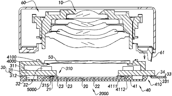
at least one molded unit, wherein the molded unit comprises a back surface molded portion;
at least one photosensitive element, wherein the photosensitive element has a photosensitive area and a non-photosensitive area surrounding around the photosensitive area; and
a circuit board, wherein the circuit board comprises at least one substrate and at least one electronic component, the substrate has a substrate front surface, a substrate back surface and at least one substrate channel, the substrate front surface and the substrate back surface correspond to each other, and the substrate channel extends from the substrate front surface to the substrate back surface; wherein the electronic component is conductively connected to the substrate; wherein a part of the non-photosensitive area of the photosensitive element is attached to the substrate back surface of the substrate, and the photosensitive element is conductively connected with the substrate, and the photosensitive area and another part of the non-photosensitive area of the photosensitive element correspond to the substrate channel of the substrate; and wherein the back surface molded portion is integrally bonded to at least one part of the area of the substrate back surface of the substrate;
wherein the photosensitive element has a chip back surface, and the back surface molded portion further embeds at least one part of the area of the chip back surface of the photosensitive element, wherein the back surface molded portion embeds at least one part of at least one of the electronic components protruded from the substrate back surface of the substrate.
|