| CPC H01L 27/124 (2013.01) [G02F 1/1368 (2013.01); G02F 1/134363 (2013.01); G02F 1/136286 (2013.01); H01L 21/02565 (2013.01); H01L 21/02631 (2013.01); H01L 21/465 (2013.01); H01L 27/127 (2013.01); H01L 27/1225 (2013.01); H01L 29/24 (2013.01); H01L 29/41733 (2013.01); H01L 29/66969 (2013.01); H01L 29/7869 (2013.01); H01L 29/78633 (2013.01); G02F 1/134372 (2021.01); G02F 2201/123 (2013.01)] | 10 Claims |
|
1. An active matrix substrate comprising:
a display area including a plurality of pixel areas and a non-display region other than the display area;
a substrate;
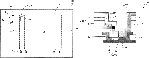
a first conductive layer being provided on the substrate, a portion of the first conductive layer working as a plurality of source lines;
a first insulating layer being provided on the first conductive layer, the first insulating layer including a first opening;
a metal oxide layer being provided on the first insulating layer, a portion of the metal oxide layer working as an oxide semiconductor layer of an oxide semiconductor TFT disposed in each of the plurality of pixel areas;
a second conductive layer being provided over the metal oxide layer, a portion of the second conductive layer working as a gate electrode of the oxide semiconductor TFT;
a second insulating layer being provided on the second conductive layer, the second insulating layer including a second opening; and
a third conductive layer being provided on the second insulating layer, a portion of the third conductive layer working as an electrode electrically connected to the oxide semiconductor TFT; wherein
the second opening is located over the first opening;
a first electrical conducting path between the first conductive layer and the metal oxide layer is in the first opening;
a second electrical conducting path between the second conductive layer and the third conductive layer is in the second opening; and
an electrically connection of the first conductive layer, the second conductive layer, the third conductive layer and the metal oxide layer is achieved by the first opening and the second opening.
|