| CPC H01L 27/1211 (2013.01) [H01L 21/823431 (2013.01); H01L 29/66795 (2013.01); H01L 29/785 (2013.01)] | 10 Claims |
|
1. A fabrication method of a fin transistor structure, comprising:
providing a first substrate, wherein a plurality of fin structures are formed on the fin structure, a dielectric layer is filled between base parts of the fin structures, and an insulation layer is at least disposed on first end surfaces of the fin structures;
disposing the first end surfaces of the fin structures on a second substrate;
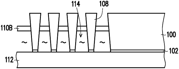
polishing the first substrate and the dielectric layer to expose the fin structures wherein the fin structures are respectively formed as a plurality of units;
removing a portion of the dielectric layer, wherein a remaining portion of the dielectric layer is a supporting dielectric layer that fixes the fin structures at waist parts of the fin structures; and
forming a gate structure layer on the supporting dielectric layer and covering a portion of the fin structures.
|