| CPC H01L 27/0924 (2013.01) [H01L 21/823431 (2013.01); H01L 29/66795 (2013.01); H01L 29/7851 (2013.01)] | 20 Claims |
|
1. A method of manufacturing a semiconductor device, the method comprising:
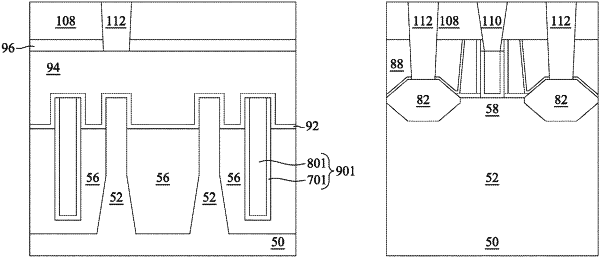
forming an opening within a dielectric material, the dielectric material being located between semiconductor fins; and
depositing a first dielectric material within the opening, the depositing the first dielectric material comprising:
pulsing a first precursor material for a first time of between about 20 seconds and about 120 seconds;
pulsing a second precursor material for a second time of between about 70 seconds and about 200 seconds, the second precursor material being different from the first precursor material;
pulsing a third precursor material for a third time of between about 20 seconds and about 120 seconds, the third precursor material being different from both the first precursor material and the second precursor material;
prior to the depositing the first dielectric material, depositing a blocking layer within the opening, the depositing the blocking layer comprising:
pulsing the first precursor material for a fourth time less than the first time;
pulsing the second precursor material for a fifth time less than the second time; and
pulsing the third precursor material for a sixth time less than the third time.
|