| CPC H01L 27/085 (2013.01) [H01L 21/0217 (2013.01); H01L 21/02164 (2013.01); H01L 21/02178 (2013.01); H01L 21/8252 (2013.01); H01L 23/291 (2013.01); H01L 23/3171 (2013.01); H01L 23/3192 (2013.01); H01L 27/0605 (2013.01); H01L 27/095 (2013.01); H01L 29/2003 (2013.01); H01L 29/205 (2013.01); H01L 29/66462 (2013.01); H01L 29/7786 (2013.01)] | 13 Claims |
|
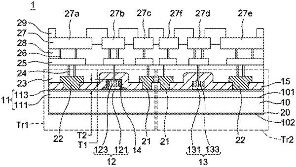
1. A semiconductor device, comprising:
a III-V material layer;
a first gate and a second gate on the III-V material layer respectively forming portions of first and second transistors, wherein the first gate comprises a first portion on the III-V material layer and a second portion on the first portion, and the first portion of the first gate comprises a first p-type doped group III-V layer, wherein the second gate comprises a first portion on the III-V material layer and a second portion on the first portion, and the first portion of the second gate comprises a second p-type doped group III-V layer; and
a first passivation layer on the first gate;
wherein a first activation ratio of an element in the first p-type doped group III-V layer of the first gate is different from a second activation ratio of the element in the second p-type doped group III-V layer of the second gate;
wherein the first and second transistors have different threshold voltages.
|