| CPC H01L 27/0711 (2013.01) [H01L 29/66234 (2013.01); H01L 29/66795 (2013.01); H01L 29/7302 (2013.01); H01L 29/785 (2013.01)] | 19 Claims |
|
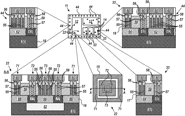
1. A method for producing a semiconductor device, the method comprising:
forming, on a substrate made from a semiconductor substance, at least one bipolar junction (BJ) transistor comprising a first terminal connected to a first well, the first well formed in the substrate and comprising a first dopant having a first dopant concentration;
forming on the substrate at least one non-BJ transistor, comprising a second terminal connected to a second well, the second well formed in the substrate and comprising a second dopant having a same polarity as the first dopant,
wherein the first dopant concentration of the BJ transistor is higher than a second dopant concentration of the non-BJ transistor; and
forming on the substrate at least an additional non-BJ transistor, different from the non-BJ transistor, the additional non-BJ transistor comprising a third terminal directly connected to a third well, the third well formed in the substrate and comprising a third dopant having (i) the same polarity as the first dopant and (ii) a third dopant concentration that is lower than the first dopant concentration.
|