| CPC H01L 27/0266 (2013.01) [H01L 27/0255 (2013.01); H01L 27/0262 (2013.01); H01L 29/0619 (2013.01); H01L 29/0684 (2013.01); H01L 29/0696 (2013.01); H01L 29/0865 (2013.01); H01L 29/1033 (2013.01); H01L 29/1095 (2013.01); H01L 29/407 (2013.01); H01L 29/4236 (2013.01); H01L 29/7397 (2013.01); H01L 29/861 (2013.01); H01L 29/8613 (2013.01); H03K 17/0828 (2013.01)] | 17 Claims |
|
1. A semiconductor device, comprising:
a semiconductor region comprising charge carriers of a first conductivity type;
a transistor cell included in the semiconductor region;
a semiconductor channel region included in the transistor cell, the semiconductor channel region having a first doping concentration of charge carriers of a second conductivity type complementary to the first conductivity type, wherein a transition between the semiconductor channel region and the semiconductor region forms a first pn-junction;
a semiconductor auxiliary region included in the semiconductor region and different from the semiconductor channel region, the semiconductor auxiliary region having a second doping concentration of charge carriers of the second conductivity type,
wherein a transition between the semiconductor auxiliary region and the semiconductor region forms a second pn-junction, the second pn-junction being positioned deeper in the semiconductor region as compared to the first pn-junction,
wherein the semiconductor auxiliary region is positioned closest to the semiconductor channel region as compared to any other semiconductor region of the semiconductor device that comprises charge carriers of the second conductivity type and that forms a further pn-junction with the semiconductor region;
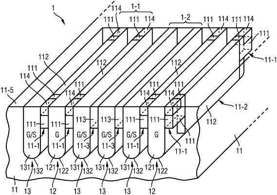
wherein the semiconductor channel region is located between a first trench and a second trench,
wherein the first trench comprises a first electrode and a first dielectric isolating the first electrode from the semiconductor body,
wherein the second trench comprises a gate electrode for controlling the transistor cell and a second dielectric isolating the gate electrode from the semiconductor body,
wherein the semiconductor auxiliary region is arranged in contact both with the first trench and the second trench.
|