| CPC H01L 27/0266 (2013.01) [H02H 9/046 (2013.01)] | 9 Claims |
|
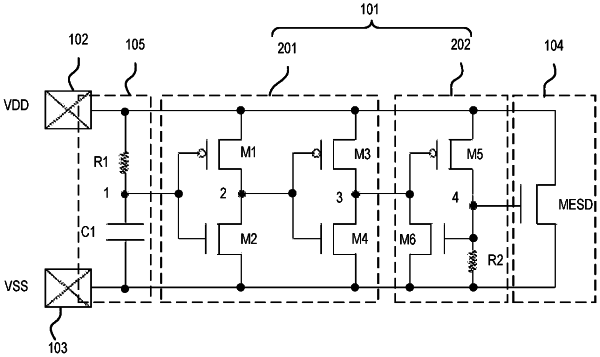
1. An electrostatic protection circuit, comprising:
a pulse detection unit configured to detect an electrostatic pulse, with a first terminal connected to a first pad, a second terminal connected to a second pad, and an output terminal outputting a detection result signal;
a discharge transistor with a gate connected to the pulse detection unit, a drain connected to the first pad, and a source connected to the second pad, the discharge transistor configured to conduct the source and the drain when static electricity happens in the first pad or the second pad, to discharge electrostatic charges; and
a processing unit connected to the pulse detection unit and the discharge transistor, the processing unit configured to control ON and OFF of the discharge transistor based on the detection result signal, the processing unit comprising: a feedback delay circuit configured to extend an ON period of the discharge transistor during the discharge of the electrostatic charges, the feedback delay circuit comprising:
a first p-channel metal oxide semiconductor (PMOS) transistor with a source connected to the first pad and a gate connected to the pulse detection unit;
a first n-channel metal oxide semiconductor (NMOS) transistor with a source connected to the second pad, a drain connected to the pulse detection unit, and a gate connected to a drain of the first PMOS transistor; and
a first resistor arranged between the gate of the first NMOS transistor and the second pad,
wherein the processing unit further comprises:
an inverter group comprising at least one inverter and arranged between the feedback delay circuit and the pulse detection unit.
|