| CPC H01L 25/50 (2013.01) [H01L 21/565 (2013.01); H01L 24/48 (2013.01); H01L 24/49 (2013.01); H01L 24/73 (2013.01); H01L 24/85 (2013.01); H01L 25/0652 (2013.01); H01L 25/0657 (2013.01); H01L 24/32 (2013.01); H01L 2224/32145 (2013.01); H01L 2224/32225 (2013.01); H01L 2224/33181 (2013.01); H01L 2224/43985 (2013.01); H01L 2224/48227 (2013.01); H01L 2224/4903 (2013.01); H01L 2224/73215 (2013.01); H01L 2224/73265 (2013.01); H01L 2225/0651 (2013.01); H01L 2225/06562 (2013.01)] | 16 Claims |
|
1. A packaging method, comprising:
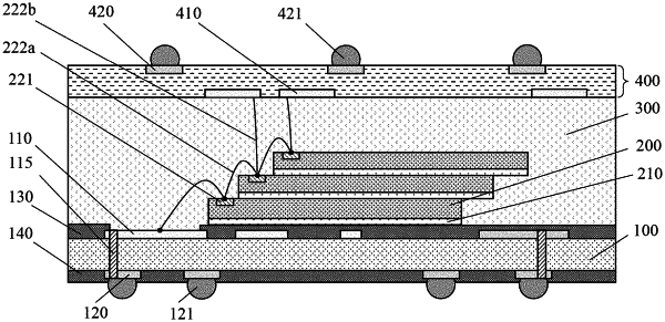
providing a substrate structure, including a core substrate, a plurality of first conductive pads at a first surface of the core substrate, and a plurality of packaging pads at a second surface of the core substrate opposite to the first surface;
packaging a plurality of semiconductor chips onto the substrate structure at the second surface of the core substrate, including:
forming a first metal wire to connect with a chip-contact pad of a semiconductor chip,
forming a plurality of second metal wires to connect chip-contact pads of the plurality of semiconductor chips to the plurality of packaging pads, wherein each second metal wire connects a chip-contact pad to one of a packaging pad and another chip-contact pad, and
forming a molding compound on the second surface of the core substrate to encapsulate the plurality of semiconductor chips and the plurality of second metal wires, wherein one end of the first metal wire connects to the chip-contact pad, and another end of the first metal wire is exposed at a surface of the molding compound; and
forming a first metal pad on the surface of the molding compound to electrically connect with the first metal wire.
|