| CPC H01L 25/18 (2013.01) [H01L 24/05 (2013.01); H01L 24/08 (2013.01); H01L 24/09 (2013.01); H10B 41/27 (2023.02); H10B 43/27 (2023.02); H01L 2224/022 (2013.01); H01L 2224/05025 (2013.01); H01L 2224/08145 (2013.01); H01L 2224/0903 (2013.01); H01L 2224/09181 (2013.01); H01L 2924/14511 (2013.01)] | 20 Claims |
|
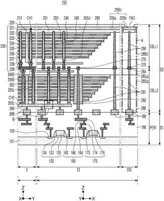
1. A semiconductor device, comprising:
a first semiconductor structure including a substrate, circuit devices disposed on the substrate, and first bonding pads disposed on the circuit devices; and
a second semiconductor structure connected to the first semiconductor structure, the second semiconductor structure including,
a base layer;
memory cell structures stacked in a direction perpendicular to a lower surface of the base layer;
at least one wiring line disposed between the memory cell structures and shared between the memory cell structures;
first and second conductive layers spaced apart from each other and disposed on an upper surface of the base layer;
a pad insulating layer disposed on the first and second conductive layers and having an opening exposing a portion of the second conductive layer;
a third conductive layer below the memory cell structures; and
second bonding pads below the third conductive layer and disposed to correspond to the first bonding pads.
|