| CPC H01L 25/167 (2013.01) [H01L 33/0093 (2020.05); H01L 33/0095 (2013.01); H01L 33/62 (2013.01); H01L 2933/0066 (2013.01)] | 20 Claims |
|
1. An integrated circuit (IC), comprising:
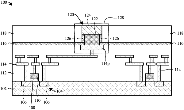
an interlayer dielectric (ILD) structure disposed over a semiconductor substrate, wherein an interconnect structure is embedded in the ILD structure;
a first dielectric structure disposed over the ILD structure and the interconnect structure, wherein a conductive pad of the interconnect structure is at least partially disposed between first inner sidewalls of the first dielectric structure;
a second dielectric structure disposed over the first dielectric structure, wherein the first inner sidewalls are disposed between second inner sidewalls of the second dielectric structure;
a sidewall barrier structure disposed over the first dielectric structure and extending vertically along the second inner sidewalls;
a lower bumping structure disposed over the conductive pad and between the second inner sidewalls, wherein the lower bumping structure extends vertically along the first inner sidewalls and along third inner sidewalls of the sidewall barrier structure; and
an upper bumping structure disposed over both the lower bumping structure and the sidewall barrier structure, wherein the upper bumping structure extends vertically along the second inner sidewalls, and wherein an uppermost point of the upper bumping structure is disposed at or below an uppermost point of the second dielectric structure.
|