| CPC H01L 25/165 (2013.01) [H01L 23/3128 (2013.01); H01L 23/367 (2013.01); H01L 23/481 (2013.01); H01L 23/49811 (2013.01); H01L 23/5384 (2013.01); H01L 23/5385 (2013.01); H01L 23/5389 (2013.01)] | 21 Claims |
|
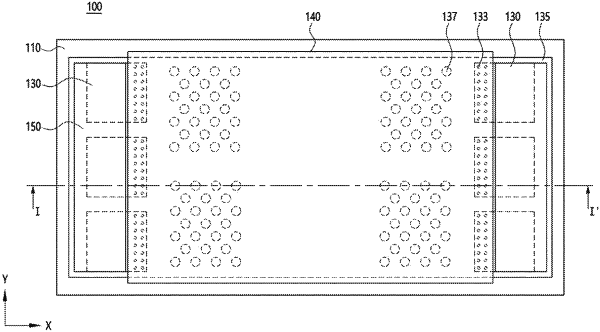
1. A semiconductor package comprising:
a package substrate;
a plurality of memory stacks disposed and spaced apart from each other on the package substrate by a predetermined distance;
at least one processor chip disposed on the plurality of memory stacks and partially overlapped with each of the plurality of memory stacks; and
one or more heat dissipation structures disposed on upper surfaces of the plurality of memory stacks,
wherein each of the plurality of memory stacks comprises an overlapped portion overlapped with the at least one processor chip viewed in a plan view and a non-overlapped portion not being overlapped with the at least one processor chip viewed in the plan view.
|