| CPC H01L 25/16 (2013.01) [H01L 21/486 (2013.01); H01L 21/4853 (2013.01); H01L 21/6835 (2013.01); H01L 21/78 (2013.01); H01L 23/3675 (2013.01); H01L 23/481 (2013.01); H01L 23/49816 (2013.01); H01L 23/528 (2013.01); H01L 23/5386 (2013.01); H01L 24/16 (2013.01); H01L 24/17 (2013.01); H01L 24/81 (2013.01); H01L 24/97 (2013.01); H01L 25/50 (2013.01); H01L 2221/68372 (2013.01); H01L 2224/16145 (2013.01); H01L 2224/16146 (2013.01); H01L 2224/1703 (2013.01); H01L 2224/17181 (2013.01); H01L 2224/81005 (2013.01); H01L 2224/95001 (2013.01)] | 19 Claims |
|
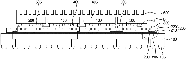
1. A semiconductor package, comprising:
a package substrate;
a first interposer substrate mounted on the package substrate;
a second interposer substrate disposed on the first interposer substrate; and
a semiconductor chip mounted on the second interposer substrate,
wherein the first interposer substrate comprises:
a first base layer;
a second base layer disposed on the first base layer, a top surface of the first base layer contacting a bottom surface of the second base layer;
a first pad exposed with respect to the first base layer at the top surface of the first base layer and connected to a first interconnection pattern which is in the first base layer;
a second pad exposed with respect to the second base layer at the bottom surface of the second base layer; and
a third pad exposed with respect to the second base layer at a top surface of the second base layer,
wherein the first pad and the second pad are connected to each other, at an interface between the first base layer and the second base layer,
wherein a second interconnection pattern of the second interposer substrate is connected to the third pad, at an interface between the second base layer of the first interposer substrate and the second interposer substrate, and
wherein the first base layer and the second base layer are each formed of silicon (si).
|