| CPC H01L 25/16 (2013.01) [H01L 21/563 (2013.01); H01L 23/315 (2013.01); H01L 23/3128 (2013.01); H01L 23/3171 (2013.01); H01L 23/5226 (2013.01); H01L 23/5283 (2013.01); H01L 24/17 (2013.01); H01L 23/293 (2013.01); H01L 2224/02373 (2013.01); H01L 2224/02379 (2013.01); H01L 2224/02381 (2013.01); H01L 2224/0401 (2013.01)] | 17 Claims |
|
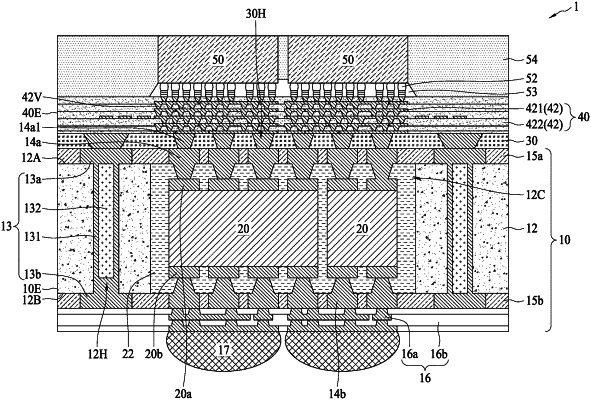
1. A semiconductor device package, comprising:
a first conductive structure comprising:
a substrate;
at least one first electronic component disposed in the substrate;
an upper dielectric layer disposed on the substrate;
a stress buffering layer disposed on the upper dielectric layer, wherein the upper dielectric layer and the stress buffering layer form an interface; and
a first circuit layer disposed on the substrate and electrically connected to the first electronic component, wherein the first circuit layer comprises a conductive wiring structure in the upper dielectric layer and the stress buffering layer, and the conductive wiring structure penetrates the interface; and
a second conductive structure disposed on the stress buffering layer and connected to the first circuit layer, wherein a coefficient of thermal expansion (CTE) of the stress buffering layer is between a CTE of the first conductive structure and a CTE of the second conductive structure.
|