| CPC H01L 25/105 (2013.01) [H01L 23/49838 (2013.01); H01L 23/5389 (2013.01); H01L 24/09 (2013.01); H01L 24/19 (2013.01); H01L 24/20 (2013.01); H01L 25/0652 (2013.01); H01L 25/50 (2013.01); H01L 23/49816 (2013.01); H01L 23/49827 (2013.01); H01L 25/0657 (2013.01); H01L 2224/0401 (2013.01); H01L 2224/04042 (2013.01); H01L 2224/04105 (2013.01); H01L 2224/12105 (2013.01); H01L 2224/32145 (2013.01); H01L 2224/32225 (2013.01); H01L 2224/48091 (2013.01); H01L 2224/48227 (2013.01); H01L 2224/73265 (2013.01); H01L 2224/73267 (2013.01); H01L 2224/92244 (2013.01); H01L 2224/97 (2013.01); H01L 2225/0651 (2013.01); H01L 2225/06548 (2013.01); H01L 2225/06568 (2013.01); H01L 2225/107 (2013.01); H01L 2225/1035 (2013.01); H01L 2225/1041 (2013.01); H01L 2225/1058 (2013.01); H01L 2924/1305 (2013.01); H01L 2924/13091 (2013.01); H01L 2924/1436 (2013.01); H01L 2924/1437 (2013.01); H01L 2924/15311 (2013.01); H01L 2924/3511 (2013.01); H01L 2924/3512 (2013.01); H01L 2924/37001 (2013.01)] | 20 Claims |
|
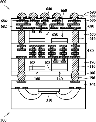
1. A package structure, comprising:
a package component;
a dummy die disposed over the package component;
a device die adjacent to the dummy die, wherein the device die comprises a conductive pad, and the conductive pad is electrically connected to the package component; and
a buffer layer formed below the dummy die, wherein the buffer layer has a first surface and an opposite second surface, the first surface is in direct contact with a bottom surface of the dummy die and the second surface is in direct contact with a package layer.
|